To create the desired circuit pattern, the excess copper is etched away using a chemical process. What remains is the intricate network of copper traces that will carry electrical signals throughout the PCB. After etching, the best pcb manufacturers in china undergoes a copper-plating process to reinforce the circuit traces and create a more durable, conductive surface.
Drilling and Component Placement:
Tiny holes are drilled into the PCB to accommodate the various electronic components, such as resistors, capacitors, and integrated circuits. These holes are precisely aligned with the design’s specifications. Once the holes are in place, the PCB undergoes a solder mask application, which protects the copper traces and ensures that solder only adheres where components need to be connected.
Soldering and Testing:
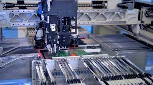
With the holes drilled and the solder mask applied, electronic components are placed on the PCB. This process often utilizes automated machines to ensure precision and efficiency. The components are then soldered in place, creating secure connections between the components and the PCB. After assembly, each PCB is subjected to rigorous testing to ensure that all connections are functioning as intended. Any defects or issues are rectified at this stage.
Conclusion:
PCB fabrication is a highly specialized and intricate process that underpins the electronic devices we rely on daily. As technology advances, the demand for smaller, more complex, and high-performance PCBs continues to grow. Understanding the intricacies of PCB fabrication sheds light on the incredible engineering and precision required to bring our electronic gadgets to life. The next time you use a smartphone, tablet, or any electronic device, take a moment to appreciate the silent heroes that make it all possible – the PCBs.